USE DISCOUNT CODEEXPERT30TO SAVE $30 USD
Autorouter not working between board regions
giacobbe_85 , 05-24-2020, 04:34 AM
I created a default Altium 20 two layers PCB and I divided it in two regions with a split line. I am able to hand route the tracks with no problems.
Anyway, in these conditions the autorouter is not able to route the two SMD components. But if I remove the split line and create only one region, the autorouter works.
How should I set up the autorouter in order to correctly autoroute the components between the two regions?
Anyway, in these conditions the autorouter is not able to route the two SMD components. But if I remove the split line and create only one region, the autorouter works.
How should I set up the autorouter in order to correctly autoroute the components between the two regions?

beamray , 05-24-2020, 04:04 PM
You should tweak rules for that.
Rules - Manufacturing- board outline clearance. Set "SPLIT" clearance to zero.
Rules - Manufacturing- board outline clearance. Set "SPLIT" clearance to zero.
giacobbe_85 , 05-25-2020, 01:11 AM
Thank you beamray for the idea. I already tried that. I also tried to set everything in Board Outline Clearance to 0, but it still doesn't work.
beamray , 05-25-2020, 01:25 AM
Please attach PCB stack up and tracers rules.
robertferanec , 05-25-2020, 01:26 AM
I do not use autorouter .. can't really help with this 

giacobbe_85 , 05-26-2020, 12:47 AM
The board is a simple two sided top and bottom board.
The autorouter is set to Altium 20 "Default Multi Layer Board". If you need more specific autorouter rules, how can I export them?
The autorouter is set to Altium 20 "Default Multi Layer Board". If you need more specific autorouter rules, how can I export them?
chitransh92 , 05-27-2020, 05:27 AM
Hello,
The regions should not create any issues while using Active route.
Ensure below conditions are met.
1. Using Active route, the stack up for all the regions is set correctly.
2. The components for which Active route is used are selected while pressing the "Alt" key (This would highlight the connections)
3. The correct layer is selected for the routing.
if these does not work then share the detail of error that you are getting.
Thank you.
giacobbe_85 , 05-28-2020, 12:47 AM
Hi chitransh92,
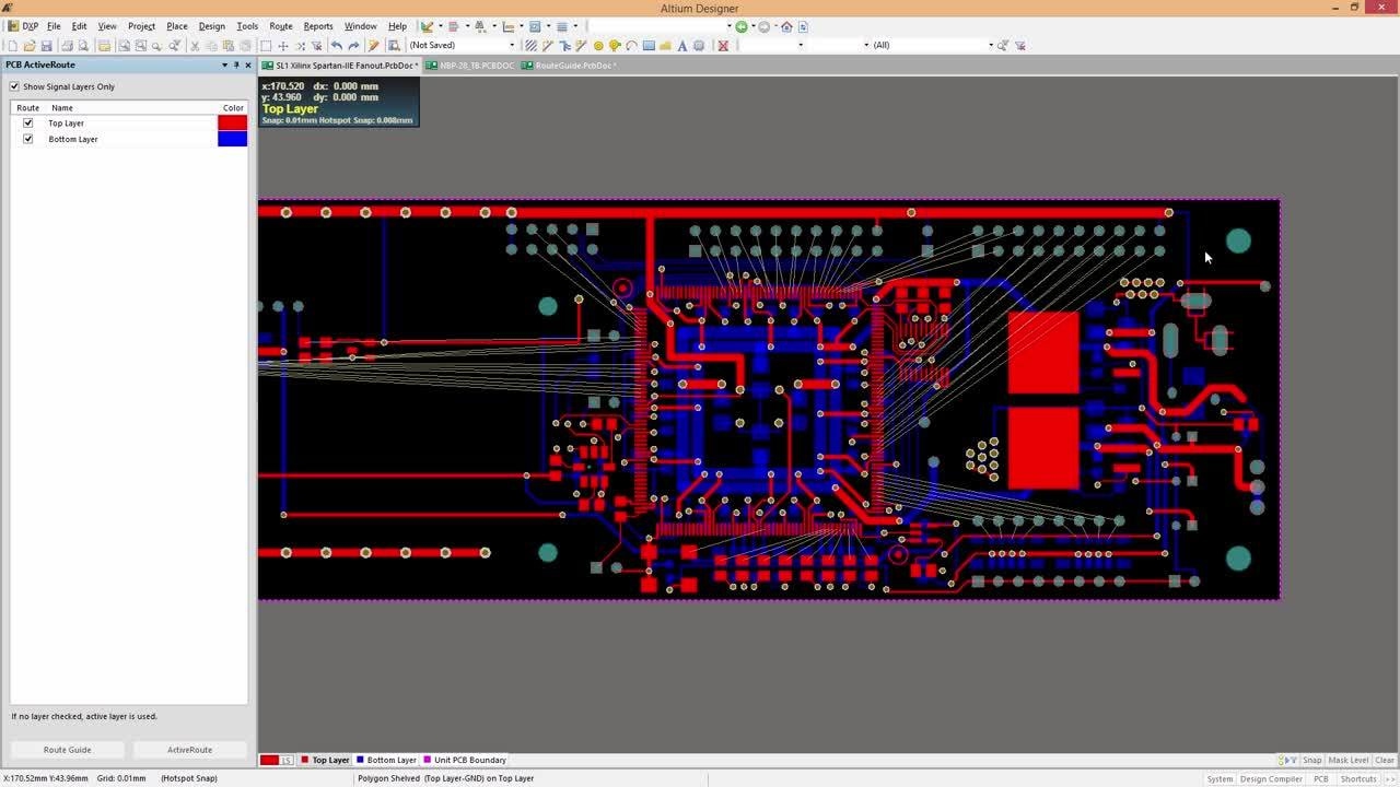
with Active Route I get the same problem of the general autorouter (Route > Autoroute > All): no tracks placed if there is a split line that divides the board in two regions. I checked your points:
1. The stackup is top-bottom everywhere, just Altium defaults;
2. I selected with the Alt key and highlighted the connections;
3. I select top layer for routing, which is the layer where the two components are placed.
Anyway, I discovered one thing: if I place the two components close to the split line, it works. See image below...

Use our interactive Discord forum to reply or ask new questions.
